Posts

Ion Beams and their Applications

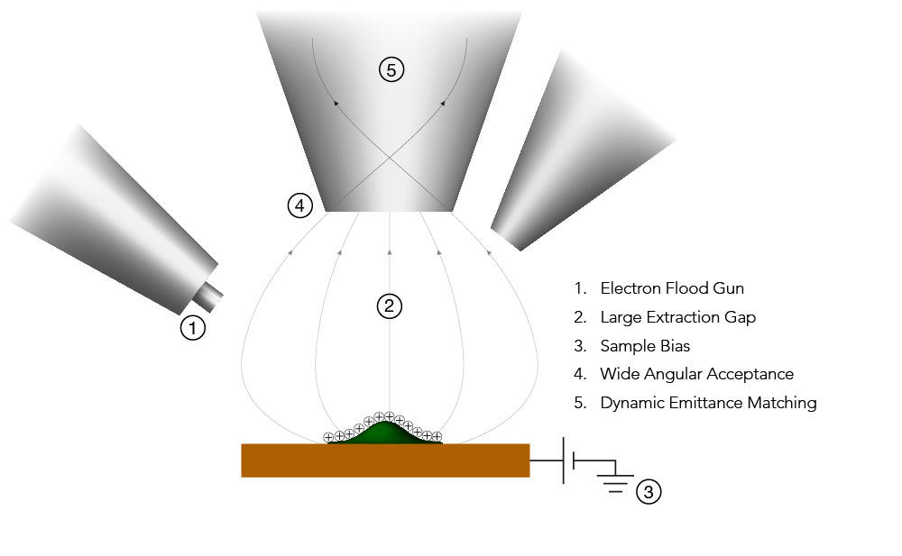
Ion beams come in many shapes and sizes, with multiple source options and applications. A minefield of options awaits if you are unfamiliar with them. This application note will shed some light on Ionoptika’s range of ion beams to help you choose the right one for your application.

Contents

  1. Sputter vs Analytical Ion Beams
  2. C60 Beams
  3. Gas Cluster Ion Beams
  4. Liquid Metal Ion Beams
  5. Plasma Ion Beams
  6. Conclusions

Sputter vs Analytical Ion Beams

We split our range of ion beams into two groups based on their applications or purpose – sputter beams and analytical beams.

Sputter Beams

While all ion beams will sputter a surface, we make this distinction based on the area and speed with which this occurs. Sputter beams have three characteristic features: high current, large spot size, and wide field of view. They deliver a large dose of ions over a wide area as quickly as possible to optimise etch rates.

Sputter beams remove material before analysis, either for cleaning purposes or for depth profiling through the sample. Techniques employing sputter beams include SIMS, XPS, SEM, TEM, and Auger.

Analytical Beams

Rather than being used to facilitate analysis using a different technique, analytical beams perform the analysis themselves. They also have three characteristic features; wide energy range, small spot size, and variable current control. These features give the user excellent control over the beam characteristics, enabling them to optimise their experiment.

Analytical beams are primarily used for secondary ion mass spectrometry (SIMS) and work well in traditional focused ion beam (FIB) applications such as secondary electron imaging and FIB milling.

C60 Beams

C60 molecule

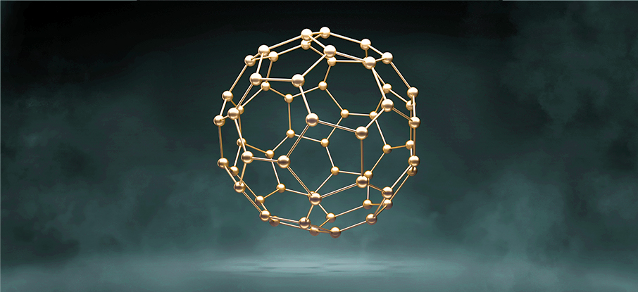
Carbon-60, or just C60, is a fullerene molecule consisting of sixty carbon atoms formed into a hollow sphere, with a shape very similar to a soccer ball. The first commercial C60 ion beam was produced in 2002 by Ionoptika in collaboration with the University of Manchester, and since then, we have sold more than 150 units worldwide.

Compared to monatomic ion beams, C60 beams result in a much “gentler” sputtering action, reducing molecular fragmentation and damage to sub-surface layers. When employed as an analytical beam, this gentle sputtering action significantly increases sensitivity to intact molecular ions.

As the C60 molecule is larger (~ 7 Å) than the lattice constant for most materials, it also does not channel through the lattice the way monatomic ions do, reducing preferential sputtering. C60 beams exhibit incredibly uniform sputter rates across a wide range of materials, including challenging poly-crystalline materials.

The properties of C60 make it suitable for both sputtering and analysis. Ionoptika offers three C60 ion beam systems: a broad-beam sputtering system, the C60-20S, and two analytical beams, the C60-20 and C60-40.

See our application note all about C60 beams for more information.

Gas Cluster Ion Beams

Illustration of a GCIB sputtering material from a surface

Gas cluster ion beams (GCIB) are high-energy beams of cluster ions, ideal for sputtering and analysing organic matter. GCIBs are an incredibly versatile ion source, as both the ion species and the beam properties can be varied, allowing the user to tune the beam to the needs of their experiment.

The source operates through the adiabatic expansion of gas in a vacuum, causing rapid cooling and cluster formation. The clusters are then ionised through electron bombardment and accelerated towards the target. The size of the cluster is a vital parameter, and users can adjust this over a wide range.

Organic Analysis

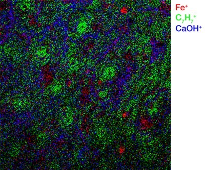
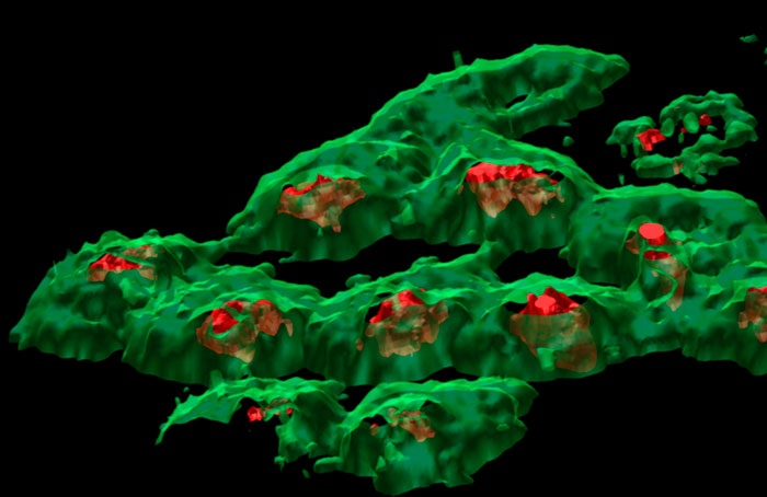
GCIBs are the ideal choice for sputtering organic matter. Etch rates of organic matter are orders of magnitude higher than for metals or semiconductors, making cluster beams such as the GCIB 10S an excellent tool for surface cleaning. The cluster distributes the ion’s energy across all constituent atoms/molecules, resulting in a very gentle sputtering effect and almost no damage to layers underneath—GCIBs perform much better than C60 on both fronts.

GCIBs must be operated at high energy to maximise their benefits for SIMS, as the secondary ion yield increases as a function of beam energy. We currently offer a 40kV variant, the GCIB 40, and a 70kV variant, the GCIB SM.

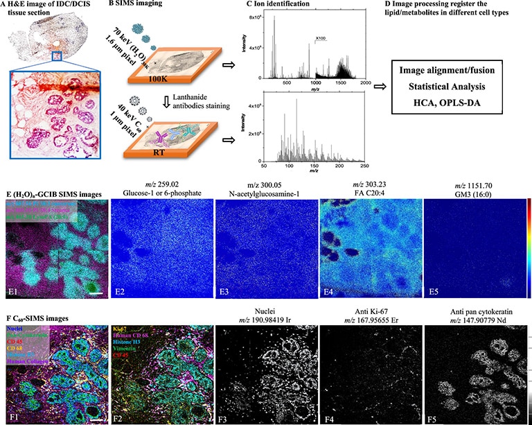
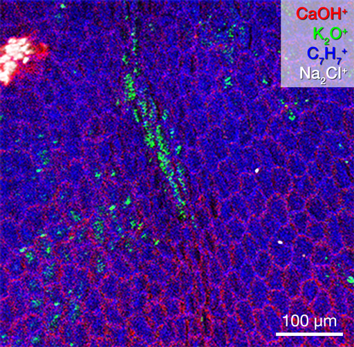
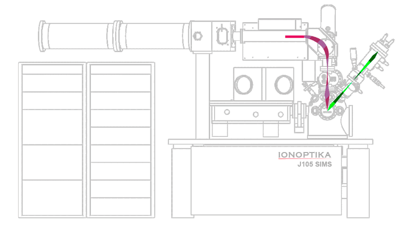
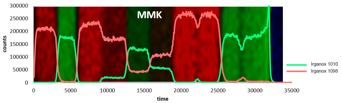
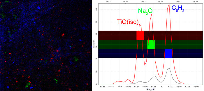
The J105 SIMS utilises the benefits of gas cluster beams for organic analysis. Combining the gentle sputter action of large cluster ions with increased secondary ion yield has extended the usable mass range to > m/z 2500.

Choice of gas

The versatility of GCIBs comes from having a choice of input gas. Argon is the most common as it is an inert gas that forms clusters easily, but Ar/CO2 mixtures and pure CO2 gas are also becoming standard for SIMS applications.

The stronger van der Waals forces between CO2 molecules result in much larger clusters than would be available for Ar – up to 20,000 in some cases. A wider range provides greater control of the all-important E/n value (energy per nucleon). Research has shown that optimising E/n results in an enhancement of the secondary ion signal. The presence of O ions at the surface may also improve the ionisation probability – further enhancing ion yield.

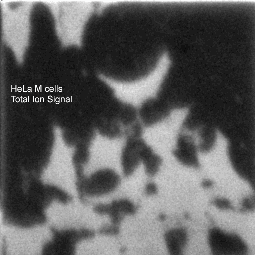
We have recently developed a GCIB source that runs on water vapour, which is currently available as an optional add-on for the J105 SIMS. Water molecules have even greater binding energy and can form enormous clusters of up to 60,000 molecules. Water clusters provide secondary ion yields up to 500 times greater than argon and are the best choice for state-of-the-art biological SIMS.

See our application note on choosing the best GCIB for your application for more detailed information.

Liquid Metal Ion Beams

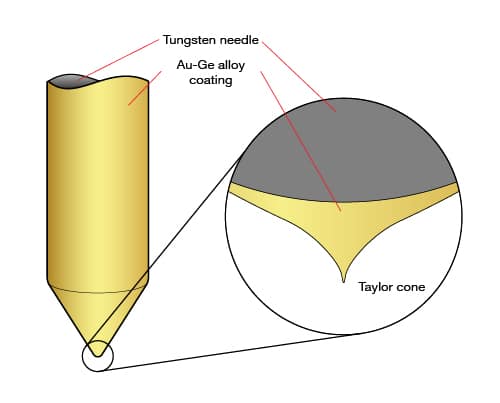
Liquid metal ion beams, also known as LMIS, or LMIG, are a well-established source technology. The source operates by a liquid metal reservoir feeding a blunt tungsten tip, from which a strong electric field extracts ions. Due to their elegant and reliable design, FIB systems have been using LMIS for decades. Ionoptika offers a 25 kV LMIG system in two variants; the IOG 25AU gold-cluster system and the IOG 25GA gallium system.

Liquid metal beams produce monatomic or small-cluster ion beams, such as Au+, Ga+, and Au3+. They feature high currents and small spot sizes (< 100 nm), making them ideal for high-resolution analysis applications.

Small, high-energy ions can penetrate far beneath the surface before dissipating their energy. Known as channelling, this causes significant sub-surface damage, making depth profiling unreliable. It also results in considerable fragmentation, making LMIS more suited to analysing hard materials.

Plasma Ion Beams

Plasma ion beam

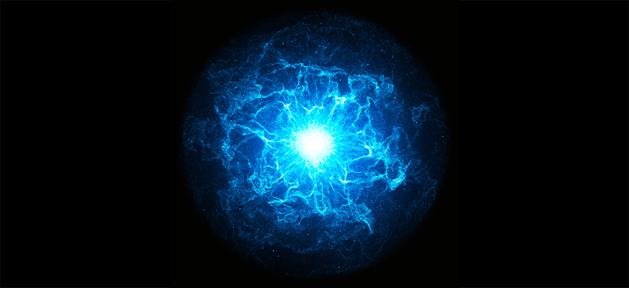
Plasma ion sources are characterised by incredibly high brightness, making them ideal for high throughput applications. A single plasma source can run on various gases without changing parts, providing flexibility. Gases available for our plasma ion beams include hydrogen, helium, oxygen, nitrogen, argon, and xenon.

Plasma sources are monatomic and do not form clusters, resulting in lower energy distributions and smaller spot sizes. Combined with their high brightness, this leads to a very high current density beam.

Plasma beams are an excellent choice where the primary goal is high-volume etching or milling. For analysis purposes, plasma beams best suit harder materials such as metals, semiconductors, and inorganics.

FLIG – Floating Low Energy Ion Beam

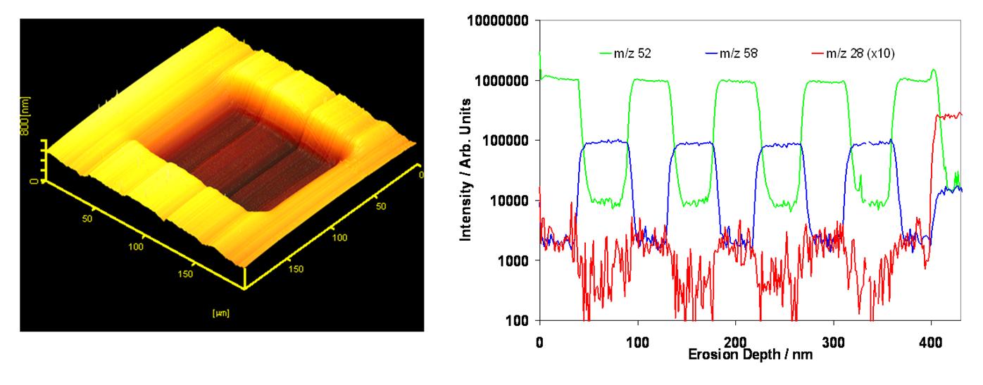
The FLIG 5 is a unique ion beam system based on a floating column design. The design enables ultra-low energy operation to 200 eV while still delivering a high current. Operating at such low impact energies significantly reduces the beam’s penetration depth, improving the depth resolution. Due to its high performance at ultra-low energies, the FLIG 5 has been the industry standard for shallow junction depth profiling for almost two decades.

Conclusion

The table below compares Ionoptika’s ion beam products under several categories discussed in this article (best viewed on desktop).

ION BEAM SPECIES ENERGY RANGE MIN SPOT SIZE BEAM CURRENT APPLICATION BEST FOR
C60 Ion Beams
C60-20S C60+, C60++, C60+++ 5 – 20 kV 100 μm 50 nA SPUTTER Organic, biological, inorganic, metals
C60-20 C60+, C60++, C60+++ 5 –20 kV 2 μm 2 nA ANALYTICAL Organic, biological, inorganic, metals
C60-40 C60+, C60++, C60+++ 10 – 40 kV 300 nm 1 nA ANALYTICAL Organic, biological, inorganic, metals
Gas Cluster Ion Beams
GCIB 10S Arn+, (CO2)n+, or (Ar/CO2)n+ 1 – 10 kV 250 μm 60 nA SPUTTER Organic & biological, polymers
GCIB 40 Arn+, (CO2)n+, (Ar/CO2)n+, or (H2O)n+ 5 – 40 kV 3 μm 200 pA ANALYTICAL Organic & biological, polymers
GCIB 70/SM Arn+, (CO2)n+, (Ar/CO2)n+, or (H2O)n+ 20 – 70 kV 1.5 μm 300 pA ANALYTICAL Inorganic, organic & biological, polymers
Liquid Metal Ion Beams
IOG 25AU Au+, Au++, Au2+, Au3+, Au3++ 5 – 25 kV 100 nm 10 nA ANALYTICAL Inorganics, metals, semiconductors
IOG 25Ga Ga+, 69Ga+ 5 – 25 kV 50 nm 20 nA ANALYTICAL Inorganics, metals, semiconductors
Plasma Ion Beams
IOG 30ECR N2+, O2+, Ar+, & Xe+ 5 – 30 kV 500 nm 500 nA ANALYTICAL Semiconductors, metals, inorganics
IOG 30D H2+, He+, N2+, O2+, & Ar+ 5 – 30 kV 500 nm 500 nA ANALYTICAL Semiconductors, metals, inorganics
FLIG 5 H2+, He+, N2+, O2+, & Ar+ 0.2 – 5 kV 15 μm 500 nA ANALYTICAL Semiconductors, depth profiling

High-resolution multi-omics profiling of individual cells

In a landmark publication, Tian et al. demonstrate the feasibility of combined GCIB/C60 SIMS imaging for multi-omics profiling in the same tissue section at the single-cell level.

A new approach

Multi-omics data are vital to understanding normal regulatory processes and are essential for designing new anti-cancer modalities. Unfortunately, sample preparation methods between different omics are typically incompatible. As such, it is nearly impossible to correlate multiple omics profiles within the same sample, let alone their spatial co-localisation at the single-cell level.

The new approach developed by Tian et al. thus represents a significant leap forward.

The study, reported in the journal Analytical Chemistry, uses a multimodal approach using the J105 SIMS to correlate different cell types. First, water cluster SIMS maps the lipids and metabolites in individual cells. Then, multiplexed SIMS imaging with a high-resolution C60 beam maps the same tissue section stained by lanthanide tagged antibodies.

Close up picture of a microscope

Multiplexed SIMS imaging involves linking specific lanthanide isotopes to antibodies and applying them to the tissue. Subsequent SIMS imaging of the lanthanides maps multiple cellular epitopes at sub-cellular resolution.

The combined approach of water cluster SIMS plus multiplexed ion beam imaging on the same tissue section enables mapping lipids, proteins, and metabolites at the single-cell level.

High-resolution multi-omics

Cryogenic water cluster SIMS was conducted on the J105 SIMS at 1.6-micron beam spot size on fresh frozen sections of invasive ductal carcinoma/ductal carcinoma in situ (IDC/DCIS) tissue. This analysis was followed by staining with lanthanide-tagged antibodies on the same frozen-hydrated tissue and imaging the same region using a C60 beam with a 1.1 µm spot size.

Workflow schematic. The frozen-hydrated IDC/DCIS sample is first analysed using water cluster SIMS with a 1.6 µm spot size. The sample is then stained with lanthanide-tagged antibodies and imaged with C60-SIMS with a 1.1 µm spot size. Image reproduced from Anal. Chem. 2021, 93, 23, 8143-8151.

The first results

Water cluster SIMS revealed the distributions and intensities of more than 150 lipids and important metabolites up to m/z 2000. HCA analysis revealed considerable variation between the location of cluster SIMS identified ions and the nine C60-SIMS cell markers.

This work represents the first successful attempt to profile proteins, lipids, and metabolites on the same tissue at the single-cell level. GCIB-SIMS, especially water clusters, has demonstrated its unique ability to detect lipids and metabolites in biological samples at unprecedented resolutions.

Picture of a person placing a sample into the J105 SIMS

Using a combined SIMS imaging approach enables the correlation of different cell types with their metabolic and lipidomic status. It offers valuable information about proteins, lipids, and metabolites on the same sample and at the same resolution.

The J105 SIMS provides a unique platform for this multimodal SIMS approach. The only instrument to offer water cluster SIMS plus multiplexed ion beam imaging, the J105 also provides high mass accuracy and tandem MS capabilities for accurate ion assignment.

Read the complete publication here.


Experience the capabilities of the J105 SIMS for yourself by booking a demonstration. Get in touch with our sales team today to organise your demo.

Why you shouldn’t overlook C60 beams just yet

C60 cluster ion beams are a fantastic tool for analyzing both hard and soft materials. Composed of sixty carbon atoms arranged into a football shape, C60 ions combine several different features making it a great all-rounder ion beam. This is why we always recommend customers to consider including a C60 beam when specifying their J105.

As the C60 molecule is larger (approx. 7 Å) than the lattice constant for most materials, it does not experience channeling the way smaller ions such as bismuth do. As such C60 beams exhibit incredibly uniform sputter rates across a wide range of materials, and even on challenging poly-crystalline materials where there is a range of crystal orientations.

As a cluster ion, C60 also produces very shallow craters with very little, if any, subsurface damage, so etch cycles are not needed to remove damaged layers when performing depth profiles or 3D imaging. As the J105 samples 100% of the analysis volume, high sensitivity is guaranteed, and combined with spot sizes as low as 300 nm, C60 is a powerful beam for delivering maximum resolution in 2D and 3D.

NiCr Standard Depth Profile C60
C60 depth profile through the NIST NiCr standard showing <5 nm depth resolution. As there is no need to perform etch cycles to remove damaged layers, depth resolution on the J105 is limited only by the crater depth of the ion beam.

The figure below shows a 3D image of a semiconductor stack alongside a depth profile through the same, performed with a 40kV C60 beam in positive ion mode. The sample consists of layers of InSb, Al, and GaAs respectively, covered in a protective photoresist layer.

3D SIMS image of InSbAlGaAs Stack with depth profil
The J105 has one mode of operation, so amazing 3D images, high-resolution 2D images, as well as detailed depth profiles can all be obtained from a single data set.

The resulting 3D SIMS image shows the layers in amazing clarity, with very sharp interfaces. As the J105 always samples 100% of the analysis volume, high sensitivity is guaranteed. The detailed depth profile through the sample also shows the presence of dissolved Al within the InSb layer, as well as the presence of Sb in the pure Al layer.

The 40kV C60 beam is ideal for this type of sample or application due to the combination of soft organic, inorganic, and hard metallic layers within the same sample. Combined with spot sizes as low as 300 nm, C60 is a powerful beam for delivering maximum resolution in 2D and 3D, no matter what type of sample you have.

Detecting pollutants in a Cherry Blossom leaf

Plant samples such as leaves are a challenging sample for ToF SIMS. Composed of insulating materials such as cellulose (cell walls) and lipophilic coatings (cuticular layer), charge build up can affect measurement quality. Using an electron gun during analysis can alleviate the charging effect and enables 3D analysis of the surface of a leaf.

Cherry blossom leaves (Prunus serrulata) collected in a busy city were analysed on the J105 SIMS using a 40 kV C60 ion beam. Pieces of blossom leaves were mounted onto double sided tape, attached to a sample stub, and gently pressed down in the corners to ensure best possible contact without deforming the leaf surface. Overview images were acquired on both sides of the leaf surface, with a spatial resolution of 1 µm per pixel and a primary ion dose of 2.2×10¹³ ions/cm2.

Experimental Conditions

Ion Beam:40kV C60+
Dose:2.2×10¹³ ions/cm2
Spatial Resolution:1 μm
Charge Compensation:60V Electron Gun, 25V Stage Bias

Without charge compensation, no secondary ions could be detected. Applying an ever-increasing stage bias would produce secondary ions temporarily. Only a combination of charge compensation methods via a 25 V pulsed stage bias and electrons emitted at 60 V beam energy enable us to generate an image of the leaf surface as well as steady signal during depth profiling.

Figure 1. Analysing the surface of a cherry blossom leaf.

Surface analysis reveals the outline of single plant cells. The outlines of the cells contain CaOH (m/z 56.97), while inorganic compounds such as K2O+ (m/z 93.92), Na2Cl+ (m/z 80.95), and Fe+ (m/z 55.93) are unevenly dispersed on the surface of the leaf. All compounds identified across the uneven leaf surface have a mass accuracy < 5 ppm (Table 1).

Analysis also revealed the surface to be coated with an even layer of organic compounds represented by molecules containing aromatic structures, e.g. tropylium ion, C7H7+ (m/z 91.05). Wax coatings on plants take the form of long aliphatic carbon chains, so aromatic structures such as these are unexpected and may indicate the presence of gasoline pollutants such as BTX (benzene, toluene, xylene).

Analysis of complex, insulating, and uneven samples such as these is made routine on the J105 SIMS.

Depth profile analysis reveals that as the cells are etched away, the layer of aromatic compounds reappears on the underside of the sample. Additionally, potassium containing substances are detected that are not present on the surface and only occur within certain cell walls (Figure 1 inset, green).

Imaging depth profile through a leaf showing CaOH (red), K2O (green), and C7H7 (blue).

Repeating the analysis on the lower epidermis reveals a high concentration of aromatic signals surrounding the stomata (Figure 2, green). It is known that plants can absorb pollutants such as BTX, mainly through the stomata, giving further evidence to the origin of these compounds.

Analysis of lower epidermis. Concentration of aromatic signals such as C7H7+ around the stomata may indicate uptake of pollutants such as BTX.

Analysis of complex, insulating, and uneven samples such as these is made routine on the J105 SIMS. Performing high-resolution 3D analysis with high sensitivity creates a more complete picture, enabling a greater understanding of the sample and its environment.

We gratefully acknowledge NESAC/BIO and the University of Washington for the use of their data in this work.

For further information about our instruments or to arrange a demonstration, please get in touch via our Contact page.

ToF SIMS of Rough or Uneven Samples

A common problem faced by TOF SIMS analysis is loss of peak resolution and mass accuracy on samples with rough or uneven topography. The J105 SIMS does not suffer from these issues, experiencing no loss in mass accuracy across even the roughest of samples

The ability to obtain consistent, accurate results is key to all analytical techniques, and none more so than ToF SIMS. Providing detailed chemical information about a surface, ToF SIMS is an extremely versatile surface analysis technique. The results, however, can be very sensitive to sample environment; insulating samples, or changes in sample height can affect the measurement and result in inconsistent, or inaccurate results.

In this application note we explain the reasons why sample roughness can be a problem, and show how the unique design of the J105 SIMS has solved this issue.

Why Roughness is a Problem for ToF SIMS

Time of flight mass spectrometers determine the mass-to-charge ratio of ions by measuring the time taken to travel a known distance under an electric field. The accuracy of this measurement – known as the mass-resolution – is determined by how precisely this flight time can be measured.

In conventional ToF SIMS, good measurement accuracy is achieved by generating very short pulses (in nanoseconds) of the primary ion beam. If the sample is completely uniform, the variation in flight time of ions with the same mass will be minimal. Thus the experiment will be quite accurate.

Say that our sample is not uniform however, but has a height variation caused by a slight tilt when mounting. In this case, ions of equal mass coming from different parts of the sample will have to travel slightly different paths, and thus will have slightly different flight times. Our experiment will not be as accurate this time, and will show broader peaks as ions of the same mass arrive at slightly different times.

What about a sample with a lot of surface roughness or height variation, such as the surface of a meteorite, or a coronary stent? In these cases it should be clear that accurate results will be difficult to obtain.

There is also a secondary issue caused by samples with rich topography, particularly those that are naturally insulating. Topographic features may result in the build up of localized surface charge. This localized charge distorts the local electric field, and can thus affect the flight path of ions at these locations.

Solving the Problem: Decoupling The Mass Spectrometer

Animated GIF of J105 SIMS Operation

Schematic of the J105 SIMS operation, illustrating the path of primary (green) and secondary (red and blue) ions through the instrument.

In order to solve this problem, the sample and its environment must be decoupled from the mass spectrometer. However, in order to do this, a new method of producing the first time-focus is required.

The J105 SIMS has been designed such that the primary beam is decoupled from the time-of-flight measurement. Instead, a shaped-field buncher and timed ion gate sit after the electrostatic analyzer, generating the first time-focus for the time-of-flight measurement. By cooling the ions prior to passing them into the buncher, the energy spread is reduced to within 1 eV, removing any effects of the sample.

As a result of this design, the distance traveled by the ions prior to reaching the spectrometer has no effect on the measured flight time. The mass spectrometer is therefore independent of the local environment on the sample.  This thus enables the J105 to analyze otherwise challenging samples, producing consistent, accurate results with no loss of resolution.

The following examples demonstrate the capabilities of the J105 to analyse rough, uneven, topographic samples without compromising mass resolution or mass accuracy.

Example #1: M1.6 Screw Thread

The figure below shows the total ion image as obtained from an M1.6 screw thread. This sample was chosen for its difficult topography, having a thread depth of approximately 300 μm. Despite the challenging nature of the sample, highly consistent results are obtained no matter what point on the surface is chosen.

The spectrum surrounding the Cr+ peak (nominally 51.94051 amu) is shown to the right of the image for a range of selected areas across the sample. The areas chosen span the full 300 μm depth of the screw thread.

Despite this large variation in height across the sample, the variation in peak center across the chosen points is only 0.0002 amu, which corresponds to a mass error of less than 5 ppm across the complete depth range.

Total Ion Image of M1.6 screw thread

Left Total ion image of an M1.6 screw thread, obtained on the J105 SIMS. Right Comparison of the Cr+ peak (nominal mass 51.94051 amu) from spectra obtained at various locations across the screw thread sample (height variation approximately 300 μm). Variation in mass accuracy across the 300 μm depth range of the sample shows less than 5 ppm deviation from the nominal value.

Example #2: Frog Embryo

The figure below shows the total ion image of a frog embryo during multiple stages of development over a 5.5 hr period. The embryo is a sphere approximately 1.1 mm in diameter – a very challenging samples for ToF SIMS.

Despite the challenging nature of the sample, uniform signal is obtained from almost all areas of the hemisphere without affecting the mass calibration.

Total ion image of developing Xenopus laevis embryo

Total ion image of a Xenopus laevis embryo at various stages of development, from 2 cells to many. Embryo is approximately 1.1 mm in diameter, in a field of view of 1200 x 1200 μm. Strong signal is obtained from all parts of the hemisphere, and the mass calibration did not change over the image. This research was originally published in the Journal of Lipid Research. Tian, H. J. Lipid Res. 2014. 55: 1970-1980. Published with permission from original author.

Conclusions

Rough, uneven, or highly topographic samples can cause problems in ToF SIMS analysis, resulting in loss of mass accuracy and mass resolution. Unfortunately, most real world samples tend not to be perfectly uniform.

The J105 SIMS solves this problem by decoupling the mass spectrometer from the primary beam, thereby removing any effects of the sample from the time of flight measurement. The result is a ToF SIMS capable of analyzing rough, topographic samples without compromising mass resolution or mass accuracy.

The J105 SIMS combines flexibility with high performance, delivering unprecedented performance on biological and inorganic samples alike. For more information, visit the J105 product page, read our Application Notes, or Contact Us to discuss your interest further.

Depth Profiling in ToF-SIMS with the J105 SIMS

Depth profiling is a powerful technique in surface analysis for examining interfaces and exploring the 3-dimensional structures of a material, to which SIMS is uniquely suited.

Many modern instruments are equipped with a sputter ion beam in addition to their primary analysis beam for depth profiling. This enables users to perform “etch-cycles” in-between analysis cycles, thereby building up a stack of 2D images and generating a 3-dimensional view of the sample.

There are limitations to the use of SIMS for depth-profiling however. Unlike non-destructive techniques such as XPS, SIMS alters the surface during analysis. In fact, fragmentation and migration of species can occur up to 20 nm below the surface. Etch-cycles therefore perform several duties. 1. They enable 3D image capture in a realistic time-frame, and 2. they remove the damaged layers, leaving behind a relatively clean surface for the subsequent analysis cycle. This process has some obvious drawbacks, most notably that a significant amount of material is lost during each cycle. This can severely limit the depth resolution.

As the J105 SIMS uses a dual-stage ToF analyzer, any beam may be employed as the primary analysis beam, including C60 and gas cluster beams. In this case, additional etch-cycles are not required – analysis and low-damage etching are continuous and concurrent. This means that no data is lost and all the material is sampled, making the J105 SIMS an extremely accurate tool for depth profile analysis.

No etch-only cycles on the J105 SIMS

As the J105 uses a DC beam, there is no need to interlace an etching beam with the analysis beam as analysis and low-damage etching are continuous and concurrent.

Organic Samples

In 2015, NPL led a VAMAS study comparing compositional analysis of an organic layered structure using both SIMS and XPS. The stack consisted of layers of Irganox 1010 and either Irganox 1098 (denoted MMK) or Fmoc-pentafluoro-Lphenylalanine (denoted MMF) in well defined ratios.

Chemical structure of Irganox 1010 and Irganox 1098

Chemical structure of (a) Irganox 1010, and (b) Irganox 1098.

Compared with a number of instruments using a Bin+ analysis beam, the J105 SIMS, using a 40 kV Ar4000+ beam, achieved the highest depth resolution of any instrument, demonstrating 12.8 nm. The figure below shows an example depth profile of such an organic stack structure.

VAMAS depth profile using J105 SIMS

Depth profile of a stacked Irganox 1010/Irganox 1098 sample. The J105 SIMS demonstrated a depth resolution of 12.8 nm – the highest of any instrument in the study.

HeLa cells

Depth profiling may also be used to produce 3D chemical maps of complex structures. The example below shows a 3D reconstruction of HeLa cells – an immortal human cervical cell line. The lipid phosphocholine head group (m/z 184.1), shown in green, represents the cell membrane, while the nucleic acid adenine (m/z 135.1), shown in red, represents the nucleus.

3D chemical map of HeLa cells

3D chemical mapping of HeLa cells using a 40 kV C60 beam. Phosphocholine (m/z 184.1 – green) and adenine (m/z 135.1 – red) represent membrane and nucleus respectively. Data courtesy of John Fletcher.

Such 3D reconstructions, detailed by Fletcher, Rabbani, and Henderson et al. here, require extensive post-processing of the data to convert the 2D layers – which have no height information – into a 3D image that is representative of the actual structure. The result, however, is a stunning reconstruction of the cell structure, that is made possible by the ability of the J105 SIMS to capture a complete spectrum from each voxel without loss of data.

The animation below reveals how the cell membrane is gradually removed to reveal the internal contents – in this case, depicted by the void created in cells.

Animated GIF of depth profile through HeLa cells with J105 SIMS

Depth profiling through HeLa cells using a 50 kV (CO2)5000+ beam at 1 μm per pixel. The lipid layer (phosphocholine) @ m/z 184.1 – representing the cell membrane, is gradually etched away, revealing the contents of the nucleus (adenine) @ m/z 135.1. Data courtesy of Hua Tian.

Inorganic Samples

The properties of poly-atomic ion beams such as gas clusters and C60+ are particularly useful for the analysis of organic samples, and have allowed molecular depth profiling to become a reality. However, that does not mean that such ion beams do not also provide benefits on inorganic samples. In fact, C60 ion beams are uniquely useful for use on both organic and inorganic samples.

Sputtering under C60+ has been shown to be less sensitive to variation in material, incidence angle, and crystallinity of the sample and has been show to offer improvements in quantitation and reproducibility on glass/mineral standards, and therefore provide an excellent solution for depth profiling on these types of samples.

NIST Ni:Cr Standard

The performance of 40 keV C60+ on a metal multilayer sample is demonstrated on the Ni:Cr standard reference material from NIST. The sample comprises alternating layers of Ni and Cr on a silicon wafer substrate. The plot on the left shows the signal from the m/z 52, and 58 mass channels corresponding to the Cr and Ni respectively. The Ni layers are 66 nm thick and the Cr layers 53 nm. A depth resolution of ca. 5 nm is calculated (16-84% rising edge of 1st Ni layer). This is close to the expected crater depth of a single C60+ impact.

Depth profile through NIST Ni:Cr standard with J105 SIMS

40 keV C60+ depth profile through the NIST Ni:Cr standard showing < 5 nm depth resolution.

Mixed Metal Oxide Sample

The example below is a depth profile through a mixed metal oxide material of relevance in hydrogen fuel cell fabrication. The experiment was performed using a C60+ 40 keV primary ion beam rastered over a 150 × 150 µm2 field of view. The J105 provides excellent signal to noise as all the material is collected during the depth profile similar to a dynamic-SIMS instrument but with the parallel mass detection and mass range of a time-of-flight analyzer. Decoupling the mass spectrometry from the ion generation process also means that the mass resolution is not compromised, and mass accuracy and calibration does not drift as the sample is eroded. Depth profiles and 3D images are generated retrospectively from the “image stack” with the outermost pixels discarded to remove any crater-wall artifacts.

Depth profile through fuel cell using J105 SIMS

Variation in secondary ion signal as a function of primary ion beam fluence for Cr+, Fe+, CeO+, and TiO+ displayed in the profile and 3D reconstruction in green, grey, red, and blue respectively. 150 x 150 μm2 field of view, z depth approximately 600 nm.

The composition of this sample is in fact much more complex than shown in the above plot and 3D rendering, and contains Al, Mn, Cr, Ce, Fe, Ti and oxides of these metals all of which are observed clearly in the mass spectra through the profile, in addition there is a thin layer of Na and K on the very surface of the sample (not shown).

Conclusions

The J105 SIMS provides an excellent solution for depth profiling of samples. The ability to use a variety of cluster beams for continuous and concurrent analysis and low-damage etching, without the need for “etch-only” cycles, enables high depth resolution on any sample type. If you would like more information, or would like to speak to a member of our team, please get in touch via our Contact page.

ToF-SIMS Analysis on Insulating Samples

Performing ToF-SIMS analysis on insulating samples can be particularly challenging. Surface charge can impact the accuracy of the results, or in the worst cases prevent any results being obtained. Thanks to its unique ToF design, the J105 SIMS is capable of imaging highly insulating samples without loss of signal or performance.

The Problem

Insulating samples provide a particular challenge for the ToF-SIMS user. A charged beam of particles impinging a surface necessarily produce a surface charge, both by emission of secondary electrons and by transfer of charge to that surface. For a metallic sample this charge is easily dissipated into the surrounding bulk, however this is not the case for insulating materials where there are no free electrons to neutralize the charge. The result is a build up of surface charge that can have a number of deleterious effects on a ToF-SIMS experiment.

For instruments where the time reference is determined by the primary beam pulse, regions of surface charge can affect the flight time of ions ejected from the surface, thereby negatively impacting on the mass-accuracy of the experiment. This effect is particularly pronounced around regions of topography where field strength is enhanced – in the worst case this leads to highly distorted fields preventing ions from ever reaching the detector. The most prominent effect of surface charge, however, is the suppression of secondary ion signals due to field suppression and/or neutralization prior to extraction.

The Solution

Thanks to its unique ToF design, the J105 SIMS is capable of imaging highly insulating samples without loss of signal or performance.

ToF Design

As the J105 does not rely on a pulsed primary beam as a time reference, temporal aberration in the extraction gap, caused by sample charging or other effects, has no impact on the mass accuracy. This enables a large extraction gap and a low extraction field, which in turn mean the extraction optics can accept ions leaving the sample up to very large angles from the normal, increasing transmission. The overall result is consistent performance across the entire sample, even those areas with lots of topography.

Insulating Sample Fig

Schematic illustration of the various means by which the J105 SIMS can compensate or accommodate charging samples.

Charge Compensation

Charge compensation/neutralization may be used to alter the effects of surface charge and improve signal on charging samples; this can be achieved by sample biasing and/or low-energy electron bombardment. In sample biasing, the sample stage is biased up to ± 100 V to compensate for the field created by the surface charge. This requires that the bias voltage is able to reach the sample surface, and so may not be effective on thicker samples or in situations where conductive tracks are prohibited.

Alternatively, pulses of low-energy electrons may be interlaced between the primary beam, in a pseudo-DC mode, to directly neutralize the charge on the surface. This has advantages in that the electrons are naturally drawn to localized pockets of charge, providing a “self-limiting neutralization” mechanism. One must be careful however, as even low-energy electron beams may result in damage to fragile organic structures. Generally speaking, in most situations, it is best to use a combination of both techniques, experimenting to find the correct balance for each individual sample.

Insulating Samples

Sodium Citrate Crystal

The figure below shows SIMS images of a single sodium citrate crystal on a substrate of double-sided tape – both highly insulating materials. Using a combination of sample bias and electron flood gun to neutralize surface charge, good signal levels are obtained from all areas without loss of mass accuracy or mass resolution, despite the highly topographic surface, enabling the identification of small micro crystals of NaCl within the sample.

Sodium Citrate SIMS image

SIMS images of a single sodium citrate crystal on double-sided tape, obtained with a 40 kV C60+ beam, showing (left) total secondary ion image, (middle) Na2OH (m/z 62.985), and (right) Na2Cl (m/z 80.95 + 82.95).

Polished Rock Surface

The second example shows a SIMS overlay image of a polished rock surface. The image is a 1 x 1 mm area, taken at 1024 x 1024 pixels using a 40 kV C60+ beam. A combination of electron flood gun, and sample bias was used in this instance, with +60 V applied to the stage in order to compensate for the effects of charging. A number of elements and minerals are identified in the image, including K, Ca, SiOH, Mn, Fe, and TiO.

SIMS image of rock surface

SIMS overlay image of a polished rock surface, imaged with a 40 kV C60+ beam. A combination of a low-energy electron flood gun and sample biasing was used to optimise imaging conditions for this insulating sample. Elements and minerals visible include: K (green), Ca (yellow), SiOH (red), Mn (cyan), Fe (white), and TiO (blue). Data courtesy of Dan Graham & Tina Angerer.

Mass Accuracy

Despite the charging nature of this sample, consistent mass accuracy is maintained across the data set. This is illustrated in the figure below, where three peaks, TiO, Na2O, and C5H2 respectively, are identified with sub 5 ppm accuracy. As evidenced by the overlay image accompanying the spectrum, all three peaks are spatially distributed throughout the sample. Spatial resolution, mass resolution, and mass accuracy all combine to make peak identification a routine procedure, even on challenging samples such as this.

Mass accuracy on insulating samples

SIMS overlay image & spectrum of polished rock surface. Even on highly insulating samples such as this, high mass accuracy (<5 ppm) is maintained at all points, enabling identification of numerous mineral fragments and organic species. Data courtesy of Dan Graham & Tina Angerer.

Conclusions

Real-world samples – where sample charging and topography are unavoidable – have always posed a challenge to reliable ToF-SIMS analysis. Now, through innovations in instrument design and engineering on the J105 SIMS, analysis of such samples is becoming routine, giving you more time to focus on solving the important problems. If you would like more information, or would like to speak to a member of our team, please get in touch via our Contact page.

Pages

C60-20S

IOG C60-40

IOG C60-20