

Applications Overview
OUR SOLUTIONS IN USE
Ion Beam Applications
ADVANCED BIOLOGICAL RESEARCH
Ion Beam Solutions for Life Sciences
At Ionoptika, we’re committed to advancing research with our innovative Ion Beam systems and instrumentation. Our technology supports ground-breaking work in biomedical, quantum, and materials sciences. We cater to a diverse range of experts, from quantum physicists to medical doctors, who demonstrate the wide applicability of our tools. Our team of physicists, engineers, chemists, and biochemists is passionate about driving new research techniques.
Ion Beams offer unparalleled advantages in the life sciences, providing crucial insights into biological and biochemical processes. Whether you are exploring molecular mechanisms of disease or studying complex biomolecules, Ion Beam solutions for life sciences enable precise and low-damage analysis.
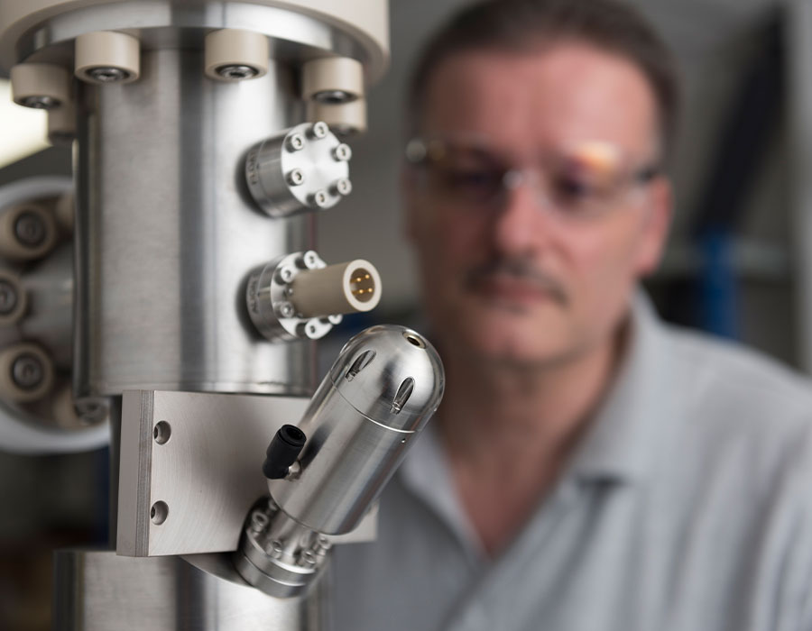
We embrace innovation.
Advanced techniques such as Gas Cluster Ion Beam Secondary Ion Mass Spectrometry (GCIB SIMS) represent a significant leap forward. GCIB SIMS provides a high-resolution analysis of delicate, large biomolecules, overcoming the limitations of traditional methods.
By utilising Gas Cluster Ion Beams, researchers can perform detailed studies on biomolecular structures with reduced sub-surface damage to fragile samples. This approach is pivotal in understanding intricate biological systems and disease mechanisms.
Explore the latest advances in GCIB SIMS and its applications in life sciences.
REVOLUTIONISING SURFACE ANALYSIS
Ion Beam Solutions for Surface Science
Surface science benefits immensely from the precision and versatility of Ion Beam technology. To conduct accurate surface and interface analysis, it’s essential to work with clean surfaces and employ sophisticated techniques. Ion Beam solutions for surface science offer a range of tools for preparing surfaces and conducting thorough analyses.
Our products are designed for your needs.
With the advent of GCIB SIMS, the J Series III has revolutionised surface analysis. This system provides exceptional spatial resolution and reduces damage to the sample, making it ideal for studying complex materials, including biological tissues and hybrid multi-layered structures. The ability to perform 3D depth profiling and high-resolution imaging simplifies the examination of intricate surface features.
Discover how our Ion Beam solutions can make surface science research easier, quicker, and more precise.
PIONEERING CHANGE AND INNOVATION
Ion Beam Solutions for Quantum Science
Quantum science is at the very frontier of technological advancement, with potential applications spanning various fields such as healthcare, communications, and financial markets. Ion Beam for quantum science play a critical role in developing quantum technologies by enabling precise fabrication and manipulation of quantum bits (qubits).
Consistency and precision in every use.
The Q-One enables deterministic single-ion implantation, which is an emerging technology for creating stable and efficient qubits. This technology meets the rigorous demands of quantum research, offering high detection efficiency and a broad range of chemical elements for implantation. As the demand for quantum technologies grows, the Q-One’s capabilities ensure that researchers have the tools necessary to overcome challenges and make significant strides in the field.
Find out more about how our solutions are driving progress and innovation in this exciting domain.
UNMATCHED ACCURACY AND CONSISTENCY
Ion Beam Solutions for Materials Science
Ion Beam technology has a range of materials science and testing applications, from etching and polishing to nanofabrication and analysis. Materials science and testing applications benefit from the versatility and precision of Ion Beams, which are essential for both fundamental research and practical applications.
Comprehensive solutions for materials analysis.
The J Series III may be configured with various Ion Beams and advanced features like high-resolution imaging, making it a valuable asset in exploring materials’ properties. Whether analysing polymers, nanotechnology, or complex hybrid materials, it excels.