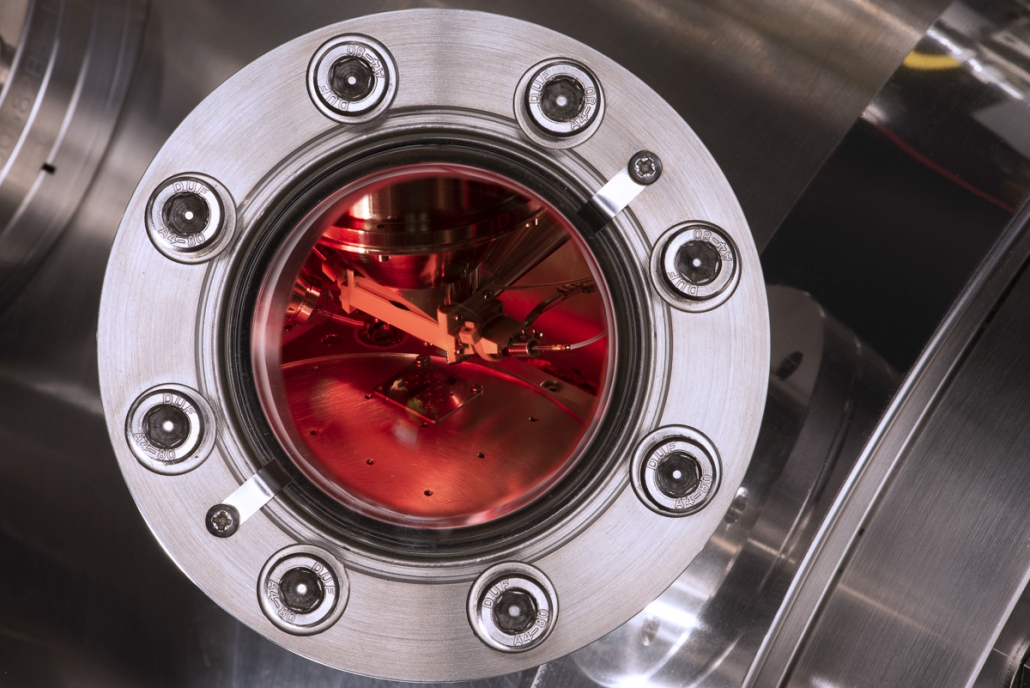
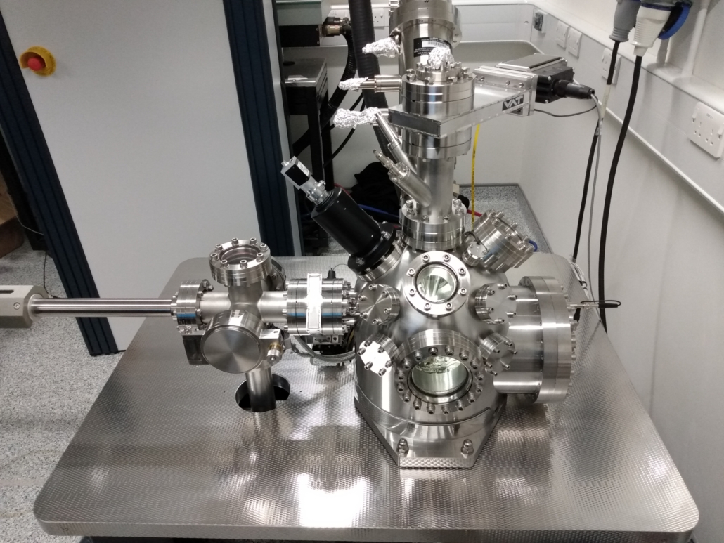
The J105 SIMS at the Rosalind Franklin Institute
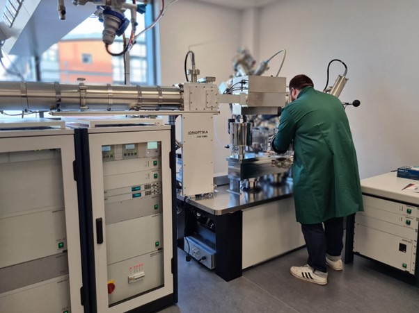
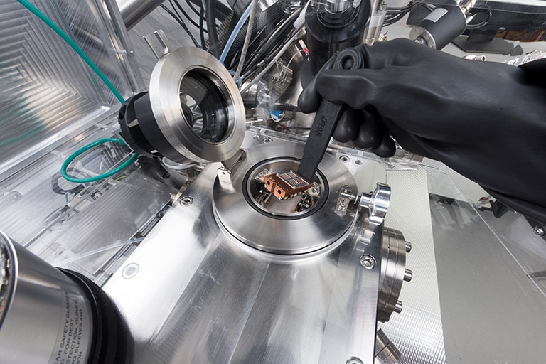
After a concerted effort of moving and installation, one of Ionoptika’s J105 SIMS instruments has found its new home at the Rosalind Franklin Institute (Franklin) in Harwell Campus.
The Franklin is a national research institute, dedicated to tackling health research challenges through the development of new technologies. One of their fields of research is Biological Mass Spectrometry, with Dr Felicia Green overseeing this particular project.
Application of the J105 at the Franklin
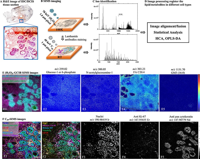
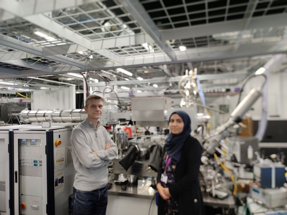
Before the building of the Franklin was completed, the J105 was installed in Manchester University, in Professor Nick Lockyer’s group. Its high sensitivity has enabled the observation of large biomolecules and their multiple charge species, never previously observed. Additionally, work performed by Prof Lockyer and Dr Sadia Sheraz in Manchester, on coupling the J105’s capabilities with laser post-ionisation, opens up a new field of research into boosting sensitivity of low abundance analytes.
Now, the Franklin will apply this ability in producing 3D SIMS images of tissue samples while maintaining structural biomolecular information.
The future of this collaboration
We are excited to see the broadening range of applications and collaborations across the Franklin and further afield that this new facility will facilitate, developing and making use of high sensitivity and sub-cellular mass spectrometry imaging at cryo-temperatures. Additionally, moving the J105 into the mass spectrometry laboratory at the Franklin will enable the use of complementary MS techniques. This will help explore and validate the –omics information produced in ToF-SIMS processes and continue developing post ionisation to further enhance sensitivity.
Commenting on the move of the J105 to the Franklin, Dr Felicia Green stated:
“We are excited by the arrival of this unique instrument. Following on from the work at Manchester we believe it has great scope to enable a broad range of research across multiple Franklin areas”.
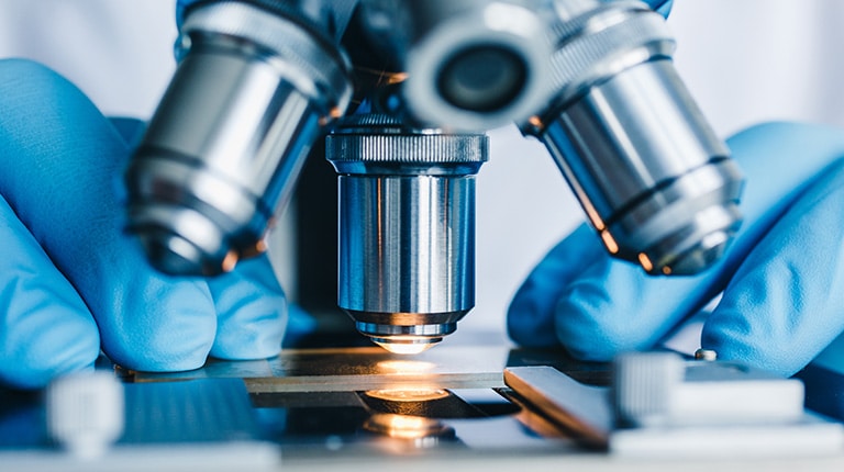
State-of-the-art mass spectrometry methods have become essential in understanding the nature and interactions of molecules in an organism. Ionoptika is extremely proud that the J105 will be able to further contribute to Franklin’s in this growing field.