Posts

What is Ion Implantation?

Ion implantation is a process whereby dopant ions are accelerated in intense electrical fields to penetrate the surface of a material, thus changing the material’s properties.

An essential technique in the semiconductor industry, it is used for modifying the conductivity of a semiconductor during the fabrication of integrated circuits. It is also heavily used for making silicon-on-insulator devices and in many other industries, including physics, materials science, and metallurgy.

Virtually all ion implantation applications involve implanting vast numbers of ions over a large area to modify the bulk properties of a material. In contrast, Q-One is designed for implanting single ions with extremely high precision to fabricate quantum devices. However, many of the same concepts apply.
Ion Implanters

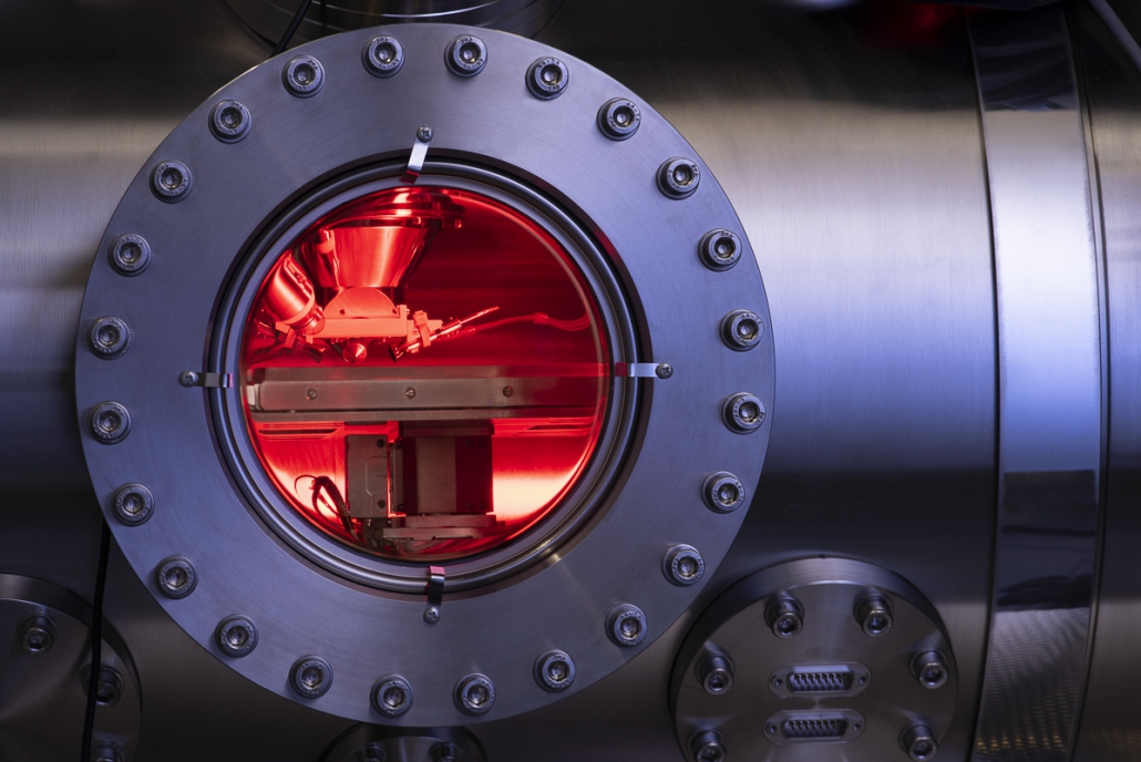
Ion implanters consist of a source region that forms the ions, an accelerator region that electrostatically accelerates them to high energy, and a target chamber. Instruments must be pumped to a high vacuum to prevent contamination of the target and breakdown under high voltage.

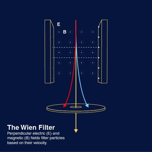
Ion sources often generate multiple ions depending on design, including different elements, their isotopes, and multiple charge states for each. A magnetic filter, also known as a Wien filter, is often used to select specific ions based on their velocity.
The implanting species, also called dopants, vary considerably with the application. Boron, arsenic and phosphorous are the most common dopants in semiconductor applications, while oxygen and nitrogen are used to process metals. Dopants for quantum applications include phosphorous,1 nitrogen,2–5 silicon,6–8 and germanium,9, and rare earth elements such as erbium.10

Implanters are often categorised by the ion beam current at the target, either low, medium or high. High-current systems for commercial applications operate at up to tens of milliamps and process hundreds of wafers per hour. On the other hand, Q-One operates at extremely low currents when implanting single ions, often tens of femtoamps.11

The ion dose is the integral of the ion current per unit area over time, measured in ions per square centimetre (ions/cm2). The dose determines the concentration of the dopant in the target. Common dose values are in the range 1016 – 1018 ions/cm2.

Beam Energy & Ion Stopping

The energy of the ion beam is a crucial parameter in ion implantation processes as it has several significant effects. The energy is the product of the accelerator voltage and the ion’s charge state, measured in electron volts (eV). For example, a Bi2+ ion accelerated in a 30 kV field has an energy of 60 keV.

Ions hitting a target lose their kinetic energy through collisions with the nuclei and electrons of the material until they stop. The depth to which the ions penetrate depends on their energy and mass, the target mass, and the beam’s angle to the crystal plane in the case of a single crystal. Higher energies penetrate further for a given mass, while lighter elements penetrate further than heavy elements for a given energy.12

The energy range of ion implantation instruments can range from 1 keV to several MeV. Q-One operates in the range of 5 – 30 kV, with an option to extend this to 40 kV. In this range, the ions penetrate approximately 5 – 100 nm beneath the surface – suitable for most quantum applications.
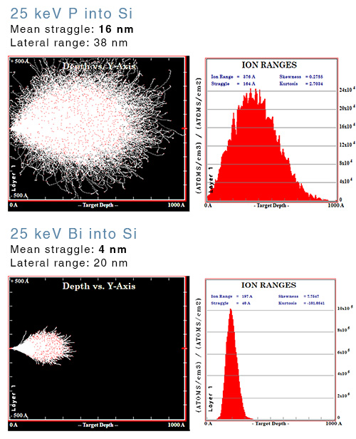
Comparison of SRIM simulations of phosphorous and bismuth implanted into silicon at 25 keV.13 Bismuth penetrates the target less than phosphorous but shows far less straggle due to its higher mass. Courtesy of the University of Surrey.

As the ions stop, they become laterally displaced from their initial trajectory, known as straggle. Straggle is an important consideration when it comes to single-ion implantation. The precision with which ions are positioned is the sum of the beam diameter at the target plus the lateral straggle. In some instances, the straggle is much larger than the beam and, therefore, the limiting factor.

Straggle is proportional to the energy and inversely proportional to the mass. So lowering the implantation energy and selecting heavier elements results in greater precision by reducing the straggle.

Damage

Ion implantation is a violent process. The projectile transfers a large amount of its kinetic energy to the target atoms, displacing them from the lattice sites. The primary collisions result in secondary collisions, and so on, in a process known as collision cascade.

The collision cascade forms a variety of defects in the material, including vacancies, interstitials, amorphous zones, stacking faults, and dislocation loops, among others.12 Thermal annealing post-implantation restores the crystalline order and allows the device to function. High temperatures can also cause diffusion of the implanted atoms, so annealing steps must be designed carefully.
Q-One Single Ion Implantation

Sputter Yield

The beam energy also has an important effect on the sputter yield. Ions impinging on a surface do not just penetrate the surface. They also sputter material, which is an important consideration, particularly at low energy.

The sputter yield (Y) is the mean number of atoms removed from the target surface per incident ion. If Y > 1, the ions remove more target material per implanted ion, resulting in erosion. If Y < 1, the ions sputter fewer target atoms per implanted ion, and material builds up. When Y = 1, there is a one-for-one replacement of target atoms with implanted ions.

Holmes et al. use TRIDYN simulations to model the sputter yield of 28Si impinging natural silicon at various energies.6 They show that the three regimes are energy-dependent and that Y = 1 at two energies, 3 and 45 keV, resulting in a planar surface. However, operating at 45 keV produces a much deeper implant and is thus more suitable for device fabrication.


Want to know more about Q-One and how it can impact your research? Get in touch with our team today, and we’d be happy to help.

References

  1. Morello, A. et al. Single-shot readout of an electron spin in silicon. Nat. 2010 4677316 467, 687–691 (2010) https://doi.org/10.1038/nature09392.
  2. Gruber, A. et al. Scanning confocal optical microscopy and magnetic resonance on single defect centers. Science (80-. ). 276, 2012 (1997) https://doi.org/10.1126/science.276.5321.2012.
  3. Naydenov, B. et al. Increasing the coherence time of single electron spins in diamond by high temperature annealing. Appl. Phys. Lett. 97, 242511 (2010) https://doi.org/10.1063/1.3527975.
  4. Brouri, R., Beveratos, A., Poizat, J.-P. & Grangier, P. Photon antibunching in the fluorescence of individual color centers in diamond. Opt. Lett. 25, 1294 (2000) https://doi.org/10.1364/OL.25.001294.
  5. Mizuochi, N. et al. Electrically driven single photon source at room temperature in diamond. Nat. Photon. 6, 299 (2012) https://doi.org/10.1038/nphoton.2012.75.
  6. Holmes, D. et al. Isotopic enrichment of silicon by high fluence 28Si- ion implantation. Phys. Rev. Mater. 5, 014601 (2021) https://doi.org/10.1103/PhysRevMaterials.5.014601.
  7. Wang, C., Kurtsiefer, C., Weinfurter, H. & Burchard, B. Single photon emission from SiV centres in diamond produced by ion implantation. J. Phys. B At. Mol. Opt. Phys. 39, 37 (2006) https://doi.org/10.1088/0953-4075/39/1/005.
  8. Neu, E. et al. Single photon emission from silicon-vacancy colour centres in chemical vapour deposition nano-diamonds on iridium. New J. Phys. 13, 025012 (2011) https://doi.org/10.1088/1367-2630/13/2/025012.
  9. Iwasaki, T. et al. Germanium-Vacancy Single Color Centers in Diamond. Sci. Reports 2015 51 5, 1–7 (2015) https://doi.org/10.1038/srep12882.
  10. Yin, C. et al. Optical addressing of an individual erbium ion in silicon. Nat. 2013 4977447 497, 91–94 (2013) https://doi.org/10.1038/nature12081.
  11. Cassidy, N. et al. Single Ion Implantation of Bismuth. Phys. status solidi 218, 2000237 (2021) https://doi.org/10.1002/pssa.202000237.
  12. Rimini, E. Ion Implantation: Basics to Device Fabrication. Ion Implant. Basics to Device Fabr. (1995) https://doi.org/10.1007/978-1-4615-2259-1.
  13. Ziegler, J. F., Ziegler, M. D. & Biersack, J. P. SRIM – The stopping and range of ions in matter (2010). Nucl. Instruments Methods Phys. Res. Sect. B Beam Interact. with Mater. Atoms 268, 1818–1823 (2010) https://doi.org/10.1016/j.nimb.2010.02.091.

New funding boosts the UK’s future in Quantum manufacturing

Q-One single ion implantation

Ionoptika Ltd and the University of Surrey have been awarded project grants worth a total of £425,000.00 from Innovate UK, the UK’s innovation agency, to expand their research into new manufacturing technologies for quantum devices.

Quantum technologies are expected to create impact across multiple sectors from more secure online communications to personalised medicine. However, to date only a handful of companies, such as IBM and Google, have successfully built a basic quantum computer because of the extreme challenges to manufacture and operate these devices. This new Innovate grant will open up new scalable manufacturing methods to researchers in the UK and around the world.

The project, entitled “Rapid and Scalable Single Colour-Centre Implantation for Single Photon Sources”, was recommended for funding by a panel of independent assessors, who concluded that “This is an innovative project by two expert partners. If it is successful, it will lead to a unique product that may possibly revolutionise quantum computing.”

Ionoptika Ltd, together with the University of Surrey, will use beams of ionised atoms to create quantum devices one at a time using rare earth elements such as erbium and ytterbium. Ion beams are used widely in the scientific and manufacturing sectors, from the production of computer chips to medical diagnostic instrumentation and cancer treatment.

The technique, known as ion implantation, has been used for decades to make modern computer chips and benefits from being much quicker than other manufacturing methods. The main limitation of the technique for quantum applications has been the inability to precisely control the location and numbers of implanted ions at the single-ion level. The new tool from Ionoptika, called Q-One, solves this problem yet is still fast enough to implant one thousand quantum bits (qubits) every second.

Q-One Single Ion Implantation

The funding comes on the back of $1.3bn in UK government funding allocated for quantum technologies research.1 It is expected to help Ionoptika expand, creating 20+ highly skilled STEM jobs in the Southampton area over the next 5-10 years, and injecting £6m+ into the UK engineering supply chain.

Paul Blenkinsopp, Managing Director at Ionoptika, commented, “Quantum technologies are set to drive the next generation of innovation and technologies. Ionoptika is delighted to be working with the University of Surrey on developing the tools and infrastructure that will be needed to realise many of these exciting quantum applications.”

Dr David Cox, from the University of Surrey, added, “The University of Surrey through the National Ion Beam Centre is delighted to work on this project with Ionoptika. The ability to precisely control the implantation of ions at the single-atom level offers enormous potential to the newly emerging quantum technologies that are set to revolutionise the world.”

Press release: pressat.co.uk/releases/new-funding-boosts-the-uks-future-in-quantum-manufacturing-766391c0ab7bf7129d63a0993739e010/


Ionoptika, a UK SME based in Chandler’s Ford, Hampshire, has driven innovation in scientific instrumentation for 27 years. Manufacturing state-of-the-art ion beam systems for labs around the world, they have contributed to research from fields as diverse as cancer research to quantum computers. For more information visit www.ionoptika.com.

1https://www.qureca.com/overview-on-quantum-initiatives-worldwide-update-mid-2021/

RADIATE: Research And Development with Ion Beams – Advancing Technology in Europe

RADIATE logo

Ionoptika has joined forces with 14 partners from public research and 3 other SMEs for the RADIATE project, exchanging experience and best practice examples in order to structure the European Research Area of ion technology application.

Besides further developing ion beam technology and strengthening the cooperation between European ion beam infrastructures, RADIATE is committed to providing easy, flexible and efficient access for researchers from academia and industry to the participating ion beam facilities. About 15,800 hours of transnational access in total is going to be offered free of charge to users who successfully underwent the RADIATE proposal procedure.

Joint research activities and workshops aim to strengthen Europe’s leading role in ion beam science and technology. The collaboration with industrial partners will tackle specific challenges for major advances across multiple subfields of ion beam science and technology.

RADIATE aims to attract new users from a variety of research fields, who are not yet acquainted with ion beam techniques in their research, and introduce them to ion beam technology and its applicability to their field of research. New users will be given extensive support and training.

The project is monitored by an External Advisory Board for quality assurance and guidance. Users with accepted proposals for RADIATE’s transnational access program are selected by an external user selection panel to ensure an unbiased and fair selection process.

RADIATE is building on the achievements of SPIRIT (Support of Public and Industrial Research using Ion Beam Technology), a previous EU funded project coordinated by the Helmholtz-Zentrum Dresden-Rossendorf (HZDR). SPIRIT ran from 2009 to 2013 and united 7 European ion beam centers and 4 research providers.

To learn more about RADIATE or to get involved, please visit the website.


This project has received funding from the European Union’s Horizon 2020 research and innovation programme under grant agreement No 824096

A New Tool for Quantum Device Fabrication

July 10th 2018 — A new single ion implantation tool is launched at the UK National Ion Beam Centre. Part of a 3 year project between Ionoptika and the University of Surrey and funded by the EPSRC, the new instrument will enable researchers to create new quantum devices faster than ever before.

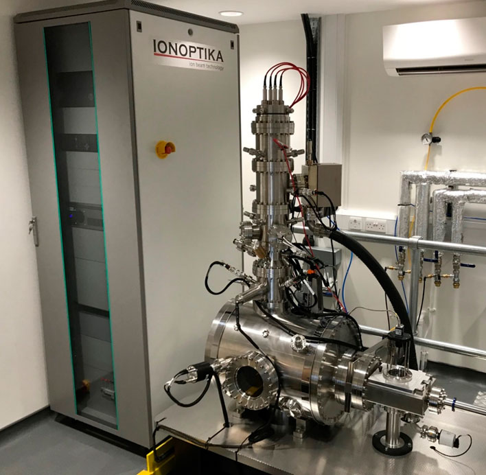
The instrument, named SIMPLE (Single Ion Multi-species Positioning at Low Energy), was launched during the 16th International Conference on Nuclear Microprobe Technology and Applications (ICNMTA2018) held at the University of Surrey (click here to read the press release).

SIMPLE Instrument

SIMPLE instrument installed at Surrey Ion Beam Centre | Photo courtesy Nathan Cassidy.

Quantum Technology

Quantum mechanics – that fascinating and sometimes bizarre theory governing the world of the very small – has enormous potential to revolutionize many aspects of modern technology. More secure digital communication, “quantum safe” cryptography methods, more accurate time measurements, and faster, more powerful computers are all thought possible.

Quantum computers in particular are an exciting prospect — it’s expected that they will be capable of solving problems not currently feasible even by our most powerful super computers. Actually building a quantum computer, however, remains an hugely ambitious challenge.

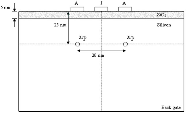
One design for a quantum bit, or qubit – the basic building block of a quantum computer – was put forward by Bruce Kane in 1998. It involves embedding pairs of donor atoms, such as phosphorous, very close to one another (~ 20 nm) within a silicon lattice. Known as electron-mediated nuclear spin coupling, the idea has been successfully utilized by researchers to fabricate individual qubits.

Qubit device schematic

Schematic of Kane’s proposed electron-mediated nuclear spin coupling qubit device.

Using a scanning tunneling microscope, researchers carefully placed individual P atoms using an atomically sharp tip and by stimulating chemical reactions on an atom-by-atom basis. An incredibly intricate technique, it can take several days of meticulous preparation to create just a single qubit. A remarkable feat, however a faster, more scalable method is clearly required.

Single Ion Implantation

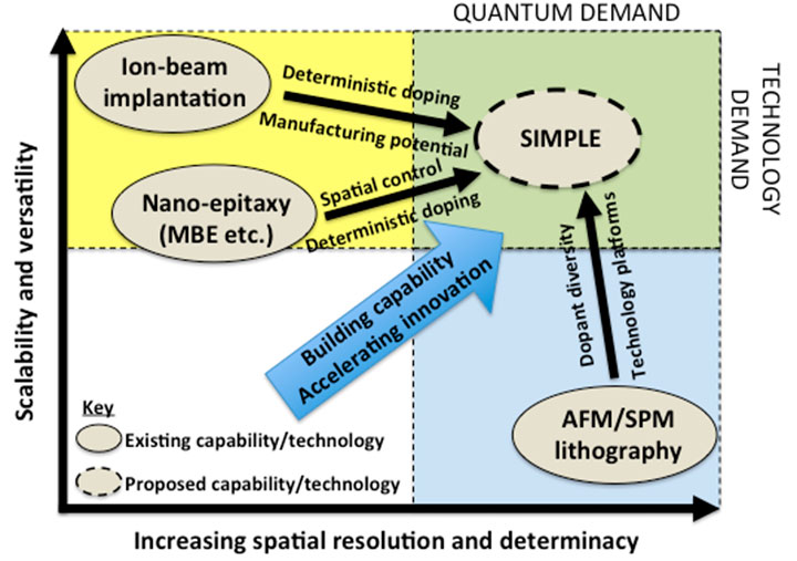
The SIMPLE project was established with this objective – to develop an instrument platform for the reliable fabrication of arrays of qubits, with high speed and high precision, using single-ion implantation.

A well established technique in the semiconductor industry, the principles of large-scale ion implantation can be applied to implant individual ions when the parameters are very carefully controlled. Leveraging Ionoptika’s expertise in ion beam design and detection, an instrument platform was designed that is capable of producing an array of millions of implanted ions in just a fraction of a second.

The need for new quantum fabrication technologies

The need for new quantum fabrication technologies


The instrument comprises a highly focused, sub-20 nm mass-filtered ion column, a nano-precision stage, and high-sensitivity single ion implantation detection system. While detecting single ion events with high enough consistency for wide scale production remains a challenge, progress in this area has been encouraging, and confidence is high that this goal will be met. And when it is, it will mark a world first, and will usher in a new era of quantum computing.


Pages

Q-One

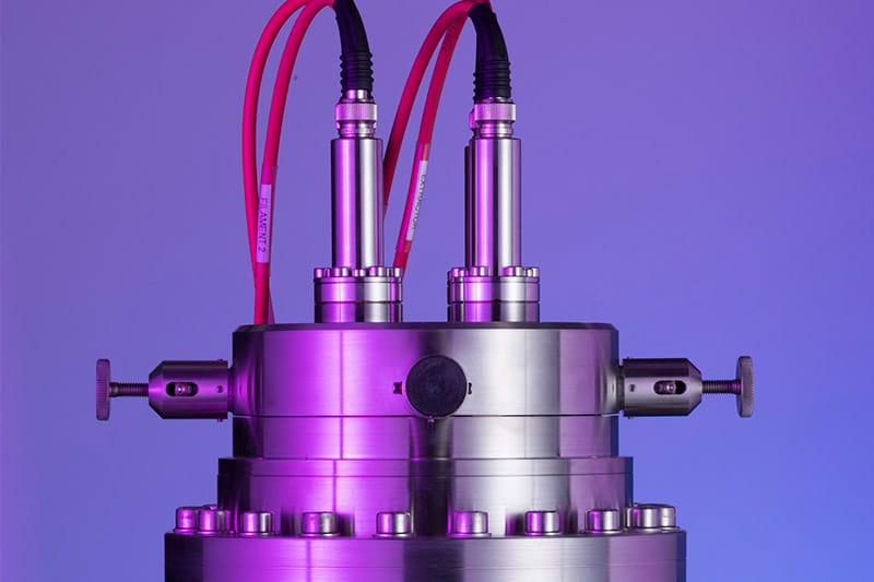
Q-One is a state-of-the-art tool for deterministic single ion implantation with nanoscale precision for quantum research and nanomaterials engineering.

Events

Nothing Found

Sorry, no posts matched your criteria