Materials Science
VARIED MATERIALS ANALYSIS
Ion Beams for Material Science
From polymers to nanotechnology, Ion Beams are employed in almost every materials science lab worldwide. Through etching, polishing, and cleaning, Ion Beams support and facilitate a wide range of analysis techniques. Other methods like SIMS and ion implantation use Ionoptika’s beams for nanofabrication and analysis.
What is Materials Science?
Unsurprisingly, Materials Science is the study of materials and how they are structured, designed, how they behave and interact; it draws on the fundamental principles of chemistry, physics and engineering to solve challenges for the future development of new technologies; from transport to medicine. The requirements of today’s technologies require materials that are stronger, lighter, more robust and cheaper than ever before.

COMPREHENSIVE SOLUTIONS
Ion Beam Solutions for a Range of Material Applications
At Ionoptika, we provide individual Ion Beams and instrumentation that are ideal for several material science applications.
Cluster SIMS
Ionoptika’s J Series III has a versatile range of features that make it ideal for materials analysis applications. The unique instrument design means that it can be used with any Ion Beam. This includes our 40 KeV C60 Ion Beam system, which is perfect for mixed materials, or our 30 IOG 30 ECR plasma source, which works best with metals or hard materials.
You can find out more about the J Series III by following the link below.
Recently, there have been exciting developments in the use of high-energy, smaller, dense clusters. Research has shown very low preferential sputtering with the 70keV GCIB used in this small cluster mode. This demonstrates its use in the analysis of Perovskites, OLEDs, glasses, and many other applications.
Developments in near-ambient pressure XPS (NAP-XPS) have led to investigations of surfaces under more real-world conditions. Primarily, this has been in the presence of gases or liquids. Ion Beams such as GCIB 10S or C60-20S are excellent additions to XPS instruments. Such Ion Beams can clean samples before analysis and provide additional depth profiling capabilities.
X-ray Photoelectron Spectroscopy (XPS)
X-ray Photoelectron Spectroscopy (XPS) is a surface-sensitive technique based on the photoelectric effect used to identify a material’s elemental composition and chemical state. It is a common material science application solution, also known simply as Photoelectron Spectroscopy (PES), and requires high vacuum conditions.
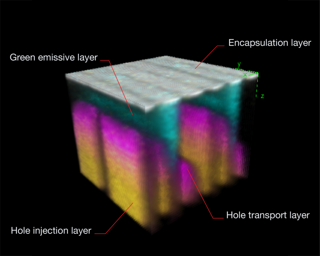
3D Imaging
A distinguishing feature of ToF SIMS is its ability to produce three-dimensional data sets. Similar to depth profiling, 3D Imaging involves repeatedly acquiring 2D images over the same area while progressively etching away material to build up a complete 3D representation of the sample. Large cluster ions are ideal for this process, as they minimise damage, enabling simultaneous etching and analysis.
Unlike techniques such as Atomic Force Microscopy (AFM), which captures a sample’s 3D topography, ToF SIMS is better suited for flat samples with layers of interest beneath the surface, such as OLED structures. While it is possible to reconstruct the topography of a non-flat sample, this requires prior knowledge of the material’s structure.