News
STAY UP TO DATE
News
Here, you’ll find everything from cutting-edge product developments to company announcements and industry insights. Stay informed on how we’re shaping the future of Ion Beam technology, and contributing to materials, life science and quantum research across the world.
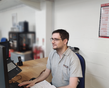
Employee Spotlight: Dr Robert Bianchini – Technical Support Engineer
Ionoptika is proud of its skilled and dedicated staff and today we're interviewing our customer support agent Dr …
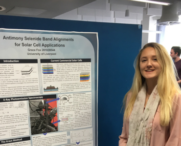
Employee Spotlight: Grace Fox – Software Engineer
Ionoptika is very proud of its skilled and dedicated staff. Today we'd like to introduce our Software Engineer …
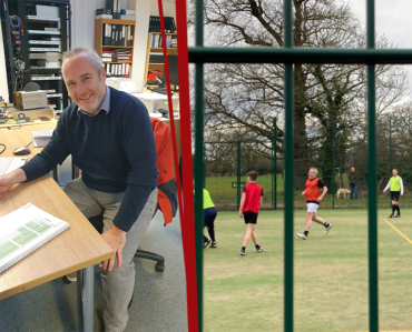
Employee Spotlight: Mark Mills – Senior Scientist
Ionoptika is very proud of its skilled and dedicated staff, who together with our loyal users make up …
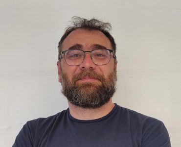
Employee Spotlight: Dr Gianfranco Aresta – Project Engineer
Ionoptika is very proud of its skilled and dedicated staff. Today, we're introducing Project Engineer Dr Gianfranco Aresta. …
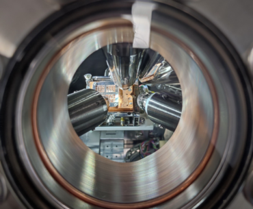
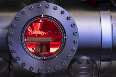
The J105 SIMS at the Rosalind Franklin Institute
One of Ionoptika's J105 SIMS instruments has found its new home at the Rosalind Franklin Institute. Find out …
What is Ion Implantation?
Ion implantation is a process whereby dopant ions are accelerated in intense electrical fields to penetrate the surface …